Goldman Sachs, China’s EUV Lithography Machine Still 20 Years Behind ASML
According to a recent report by Goldman Sachs, China has successfully developed its own version of an extreme ultraviolet (EUV) lithography machine, but the system is reportedly capable of producing only 65nm chips—a process node considered obsolete by today’s industry standards.
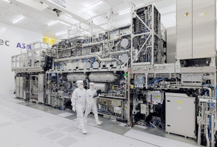
This places China’s EUV technology about 20 years behind that of Dutch leader ASML, the world’s sole supplier of advanced EUV lithography tools.
Goldman Sachs noted that while Chinese foundry SMIC has already demonstrated limited 7nm chip production, it almost certainly still relies on ASML’s older deep ultraviolet (DUV) lithography machines, given that China lacks the ability to manufacture cutting-edge EUV systems domestically.
Meanwhile, ASML is advancing into its second-generation High-NA EUV lithography, now being deployed at Intel, TSMC, and Samsung Electronics. Each High-NA EUV tool, weighing around 180 tons and the size of a double-decker bus, costs over $400 million and is essential for nodes at 1.4nm and below.
The report emphasized that it took ASML nearly 20 years and $40 billion in R&D and capital expenditures to advance EUV lithography from 65nm to 3nm and beyond, underscoring the vast gap between China’s progress and global leaders.
Goldman Sachs concluded that given China’s current semiconductor capabilities, R&D investment scale, the complexity of the global supply chain, and high geopolitical risks, it is “impossible for China’s homegrown lithography machines to catch up with advanced global standards in the short term.”
Nevertheless, Chinese media reports suggest that Huawei, with support from the Chinese Academy of Sciences and Huazhuo Precision Technology, has already entered trial production of its own EUV lithography tool in Q3 2025. The Huawei system reportedly uses laser-induced discharge plasma (LDP) technology, with the company aiming to ramp up to mass production by 2026.
댓글
댓글 쓰기